Atomistic TNL Epitaxial Material Growth CAD Software accelerates CVD deposition processes by using atomistic simulations based on physics and kinetic Monte Carlo (kMC) algorithms. This approach enables real-time replication of deposition experiments without relying on continuum models or partial differential equations.
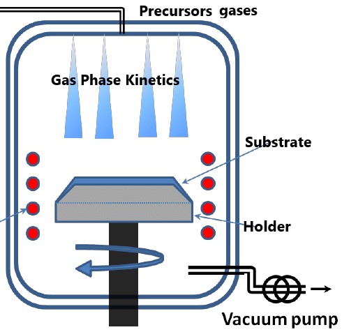
Reactor Geometry
Substrate Symmetry
Substrate Orientation
Precursors database
Carrier gases database
Flow rates
Gas phase kinetics
Surface Phase kinetics
Chamber & Substrate Temperature, Pressure
Chamber Pressure
Schwoebel-Enrich barrier
Incorporation barrier
Nearest neighbor energy
Arrehnius based chemical kinetics
Transition State Theory
Fick's law
Leonard-Jones parameters
Chapman-Enskog theory
Schmidt number
Laminar Boundary
Growth Rate
Average Surface Roughness
Lattice Parameter of each & every atoms
Average Strain
Void or Vacancy density
Interstistials density
Line defect density
Stacking Faults density
Mole fraction
Lattice Constant
Reactant gases transportation into the reaction chamber,
Reactant gases diffusion through the gaseous boundary layer to the substrate
Formation of intermediate reactants from reactant gases
Absorption of gases onto the substrate surface
Single or multi-step reactions at the substrate surface
Desorption of product gases from the substrate surface
Forced exit of undesired product gases from the system
Reliable coupled algorithms: kinetics of gas and surface phase reactions and the kinetic Monte Carlo (kMC) method
Computationally efficient to enhance the CVD deposition process and to analyze the thin film morphologies at the atomistic scale
Closed-loop operational strategy to enhance the quality of films and minimize the variability between batches due to drift
In-depth atomistic insights and understanding of chemical kinetics, including adsorption, hopping, diffusion, and desorption, with diverse output data across various input conditions
Optimize chemical kinetics and deposition parameters, including precursor and carrier gas flow rates, to improve the quality of thin films and epitaxial growth.
Reducing manpower and costs speeds up the transition from development to production for new growth processes
More details